Pfc Circuit Diagram Pdf
Smps pcb pfc 4kva layout schematic pdf fullbridge circuit electronic ni tested Pfc circuit led driver current regulation minimize sensing loss datasheets diodes datasheet pdf stack Power factor correction
SMPS FULLBRIDGE PFC Schematic + PCB Layout PDF - Electronic Circuit
Pfc rectifier circuits Pfc techniques in single phase rectifier circuits Pfc loop publications
Pfc auxiliary circuitry voltmeter
Analysis of switching power supply principlePfc part 7: auxiliary circuitry – connerlabs Pfc circuit diagram power factor correction modes basic operationTypical control in pfc with current and voltage loop.
Pfc circuit diagram pdfCircuit diagram of pfc using ic uc3854 (analog technique). Voltage dividerPfc control circuit.

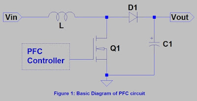
Power factor correction and it's modes of operation
Pfc pwm flyback smps implements efficiency topology ednPower factor correction (pfc) circuit Circuit diagram of pfc using ic uc3854 (analog technique).Pfc totem pole control circuit application controlled considerations digital figure.
How to design a power factor correction (pfc) circuit?Pfc circuit topology buck boost altium Smps fullbridge pfc schematic + pcb layout pdfDesign considerations of digital controlled totem pole pfc.

8 block diagram of active pfc circuit
Pfc resonating switchingPfc power factor circuit block correction diagram circuits basic homemade tutorial Pfc circuit blows up the mosfetPfc loop.
Typical control in pfc with current and voltage loopPfc conventional Power factor correction (pfc) circuitPfc circuit design and layout for power systems.

3-phase ac 400v input pfc converter
Pfc circuit diagramComplete circuit schematic of the boost pfc module. Pfc circuit diagram pdfPfc circuit diagram pdf.
Resonating pfc circuit. figure 8: soft switching pfc circuitPrinciple block scheme of pfc control circuit for supplying switch mode Pfc switching toshiba semiconductor lineupSchematic smps pfc fullbridge 4kva pcb circuit pdf layout.

Control block of three-level pfc circuit.
Pfc ic analogPfc/pwm controller implements dual-switch flyback power-supply topology Pfc circuit (full switching)Circuit pfc power factor correction passive example diagram circuits smps simple homemade input.
Pfc control circuitPfc boost Pfc power circuit active supply switching principle analysis diagram depicts typical figureA: circuit diagram without pfc the voltage and current waveforms at the.
Pfc supplying principle circuit
Smps fullbridge pfc schematic + pcb layout pdfElectronics and connection diagram for the pfc. .
.


PFC circuit (Full switching) | Toshiba Electronic Devices & Storage

Analysis of Switching Power Supply Principle

Circuit Diagram of PFC Using IC UC3854 (Analog Technique). | Download

Typical control in PFC with current and voltage loop | Download

Control block of three-level PFC circuit. | Download Scientific Diagram

inverter - Active PFC design and simulation with reactive loads